Everyone talks about AI chips. Fewer people talk about what those chips are mounted on — the printed circuit board that connects every chip to every other component inside every electronic device ever made. Six in ten circuit boards in the world today are manufactured in China. For AI data centres, that share is close to all of them. This is the supply chain story the semiconductor industry would rather not discuss.
Contents
- What a printed circuit board actually is — and why it matters now
- The market: from commodity to critical infrastructure
- How the US lost its lead: from 30% to 4% in 25 years
- The national security case: kill switches, missile guidance, and data theft
- How PCBs are actually made: a 1,000-step process
- The US vs China manufacturing gap
- The policy response: the Protecting Circuit Boards Act
- Who is rebuilding — and what it will take
What a printed circuit board actually is — and why it matters now
A printed circuit board is the substrate layer that sits beneath every semiconductor chip inside every electronic device — from wireless earbuds to fighter jets to the two-tonne server racks that power the world’s most advanced AI models. It provides the physical foundation onto which chips are mounted, and the etched pathways through which those chips communicate with one another and with the broader system. No chip, regardless of how advanced, can operate without first being connected to a board.
For most of the technology industry’s modern history, circuit boards were treated as a background commodity — an unglamorous but necessary component that attracted little strategic attention compared with the semiconductors mounted on top of them. That era is over. The explosion of AI computing demand, combined with the geopolitical pressure of ongoing conflicts and mounting concerns about supply chain integrity, has elevated the printed circuit board from an afterthought to one of the most consequential chokepoints in the global technology supply chain.
The core vulnerability: Nearly all printed circuit boards used in AI data centres — by companies including Nvidia, Google, and Apple — are currently manufactured in China. The US Department of Defense is prohibited by law from sourcing circuit boards from China. Yet the commercial AI industry, which drives the majority of PCB demand, faces no equivalent restriction — and cost and capacity continue to pull procurement toward Asia.
The market: from commodity to critical infrastructure
The global printed circuit board market has undergone a remarkable revaluation over the past two years. An industry that was historically described as commoditised — low-margin, volume-driven, and geographically concentrated in Asia — is now one of the fastest-growing segments of the technology hardware sector. Two forces are driving that acceleration simultaneously: the insatiable power demands of AI infrastructure, and the surge in military procurement driven by active conflicts in Ukraine and Iran.
The PCB market — key figures
Global PCB market (2026 projected)
$96B
Global PCB market (end of decade)
$123B
PCB industry growth rate (2026)
12.5%
PCB price increase (Mar–Apr 2026)
Up to 40%
TTM price increases signalled
5–25%
China’s share of global PCB supply
~60%
The convergence of AI data centre buildout and defence procurement is creating a demand environment that the existing global supply chain was not designed to accommodate. PCB prices reportedly climbed by as much as 40% between March and April 2026 alone. TTM Technologies, the largest US-based circuit board manufacturer, has signalled price increases of between 5% and 25% across its product lines. The commercial sector — particularly hyperscale cloud operators and AI hardware companies — is willing to pay substantially elevated prices to secure capacity, which in turn drives prices higher across all segments including defence procurement.
The PCB industry also reached a new level of financial visibility when Nvidia supplier Victory Giant Technology debuted on the Hong Kong stock exchange in April 2026 at a valuation of approximately $2.6 billion — the city’s largest listing in seven months, and a signal that circuit board manufacturers are no longer an overlooked corner of the semiconductor supply chain.
How the US lost its lead: from 30% to 4% in 25 years
In the year 2000, the United States manufactured approximately 30% of the world’s printed circuit boards. By 2026, that share has contracted to around 4%. This is not a story of technological failure but of economic attrition — the gradual migration of a labour-intensive, capital-intensive manufacturing process toward lower-cost environments, accelerated by Chinese government subsidies that made it increasingly difficult for American producers to compete on price.
China’s rise to dominance in PCB manufacturing did not happen overnight. It was the product of sustained, policy-driven investment over more than two decades — preferential financing for factory construction, subsidies for raw material procurement, and government backing for the development of domestic supply chains for the specialist resins, copper foil, glass fibre, and drilling equipment that PCB manufacturing requires. The result is a manufacturing ecosystem of extraordinary scale and integration that has no equivalent anywhere in the world outside Asia.
How the manufacturing gap happened
China — what went right
- Government subsidies covering equipment, capital, and raw materials
- Factories of 100–200 PCB assembly lines with no US equivalent
- Integrated domestic supply chains for resin, copper, and glass fibre
- Significantly lower labour costs relative to the US
- ~60% of global PCB supply; ~89% of boards used by AI leaders
United States — what went wrong
- Market share fell from 30% in 2000 to ~4% today
- Only two publicly listed domestic PCB manufacturers (TTM, Sanmina)
- Single-source dependencies for critical materials like copper foil
- No domestic equivalent to the CHIPS Act for PCB manufacturing
- Higher labour and capital costs relative to subsidised Asian producers
The national security case: kill switches, missile guidance, and data theft
The security dimensions of the PCB supply chain go considerably beyond simple concerns about component quality or delivery reliability. A circuit board is not a passive piece of plastic and copper — it is an active electronic architecture containing dozens of interconnect layers, each of which can theoretically carry embedded components that are either invisible to standard inspection or deliberately designed to activate only under specific conditions.
The threat scenarios articulated by US defence and intelligence officials fall into several distinct categories. At the most severe end is what researchers describe as hardware-level sabotage — the insertion into a PCB’s layers of a component capable of receiving a signal and then altering the behaviour of the electronic system it is embedded in. In a weapons platform, this could mean the ability to redirect a missile, disrupt guidance systems, or cause a munition to fail at a critical moment.
The kill switch scenario: US defence officials have described a scenario in which adversary-manufactured circuit boards embedded in weapons systems could be remotely activated to disrupt, disable, or redirect those systems at a time and place of the adversary’s choosing. The layered, complex architecture of modern PCBs — with up to 140 individual layers in the most advanced boards — creates multiple potential concealment points for malicious components that are extremely difficult to detect even with X-ray imaging.
Beyond active sabotage, circuit boards represent a passive intelligence vulnerability. A board with embedded routing components could systematically copy and transmit sensitive data to external parties without the knowledge of the system’s operators. In networking equipment, communications infrastructure, or defence electronics, this represents a persistent intelligence collection capability that would be essentially undetectable through conventional system monitoring.
These are not theoretical concerns for the US military. Every circuit board used in a US Department of Defense system is legally required to be manufactured domestically — a restriction designed precisely to eliminate the possibility of adversary access to the board’s fabrication process. Nvidia and its assembly partners do perform physical inspection of incoming PCBs using X-ray imaging and AI-assisted anomaly detection, but security professionals acknowledge that the most sophisticated forms of hardware tampering may not be detectable through post-production inspection alone.
Four national security risks from Chinese-made PCBs
Kill switch insertion
Embedded components capable of remotely disabling or redirecting weapons systems at the adversary’s instruction.
Data exfiltration routing
Passive components that copy and transmit sensitive data without any detectable system-level activity.
Guidance disruption
Interference with missile, drone, or munition guidance systems causing unintended trajectory or detonation.
Supply chain single points
US has only one domestic copper foil supplier — disruption would halt all domestic PCB production.
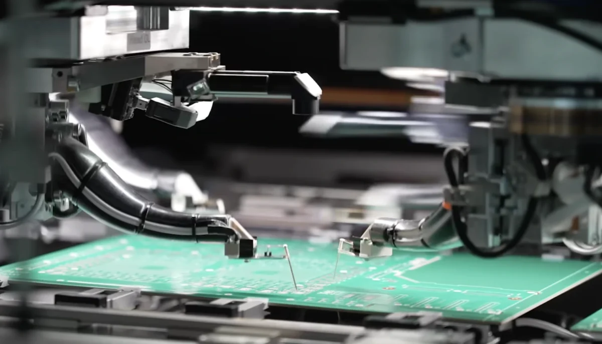
How PCBs are actually made: a 1,000-step process
The technical complexity of printed circuit board manufacturing helps explain why rebuilding domestic capacity is not simply a matter of constructing a factory and hiring workers. A single circuit board can require up to a thousand individual manufacturing steps from raw material to finished product, taking anywhere from five days for a simple consumer board to six months for the most advanced aerospace or defence-grade products.
- Copper core construction. The process begins with a copper core — a thin sheet of resin epoxy with copper foil bonded to both sides. This is the fundamental building block from which all other layers are constructed.
- Layer lamination. Up to 140 individual layers are precisely aligned and then bonded together using heat and pressure applied over three to five hours, creating a single laminated panel.
- Lithographic patterning. The circuit design is transferred onto the board using optical lithography — a patterned film or mask through which ultraviolet light etches the copper into the precise traces that form the board’s electrical pathways.
- Precision drilling. Thousands of holes are drilled through the board — using drill bits as narrow as 0.04mm, thinner than a human hair — to create the vertical interconnects that allow signals to travel between layers. Modern equipment can drill up to 100,000 holes per minute per panel.
- Copper plating and etching. The drilled holes are plated with copper to create electrical connections between layers. Excess copper is then chemically etched away to leave only the intended circuit pattern.
- Surface finishing. The bare board receives a surface treatment — which may involve gold, palladium, or immersion tin depending on the application — before chips and other components are attached in a separate assembly process.
Each manufacturing stage requires specialist equipment — presses, lasers, plating tanks, drilling machines, optical inspection systems — much of which is sourced from Japan, Germany, and Taiwan, and which carries its own lead times and single-source vulnerabilities. A breakdown at any stage can halt an entire production line.
The resource footprint: PCB manufacturing is resource-intensive at industrial scale. TTM’s global operations consumed the equivalent electricity of 70,000 homes and 2.1 billion gallons of water in 2024. The company has set targets of 60% renewable energy use and 35% water recycling to address the environmental impact of scaling production.
The US vs China manufacturing gap
The scale disparity between US and Chinese PCB manufacturing is almost impossible to overstate. TTM’s largest Chinese facility is 46 times the size of its original flagship plant in Santa Ana, California — the facility that represents the cutting edge of its domestic US capability. While a typical large US PCB factory might operate a handful of production lines, Chinese competitors routinely operate facilities with 100 to 200 simultaneous assembly lines. Nothing of comparable scale exists in the United States.
This gap reflects not only accumulated investment but an integrated manufacturing ecosystem. Chinese PCB factories can source resins, copper foil, glass fibre, specialty chemicals, drilling equipment, and plating systems from domestic suppliers at competitive prices, with short lead times. US manufacturers, by contrast, face a more fragmented and often single-source domestic supply chain — with some critical materials available from only one US supplier, creating a vulnerability that could halt domestic production entirely if that supplier were disrupted.
TTM is the only non-Asian company among the world’s 50 largest PCB makers. It and Sanmina — the only two publicly listed US-based PCB manufacturers — have seen their stock prices rise significantly over the past year as the security and supply chain arguments for domestic PCB sourcing have gained mainstream recognition. But even their combined output represents a small fraction of what the US economy would need to meaningfully reduce its dependence on Chinese-manufactured boards.
The policy response: the Protecting Circuit Boards Act
Congress has begun to move. In May 2026, legislators from both parties introduced the Protecting Circuit Boards and Substrates Act — a bipartisan bill that offers a 25% tax credit to companies that choose US-manufactured circuit boards, while a companion bill in the House provides for $3 billion in grants to support domestic PCB manufacturing expansion. The legislation is explicitly modelled on the logic of the CHIPS and Science Act, which committed $52.7 billion to domestic semiconductor manufacturing in 2022.
The financial comparison, however, illustrates both the opportunity and the limitation. While semiconductor fabs cost $10 billion or more to construct, a new PCB factory typically costs between $250 million and $400 million — meaning the capital requirements are genuinely manageable if the policy incentives are sufficient to make domestic sourcing economically competitive with China-based supply.
html
Who is rebuilding — and what it will take
TTM is making its largest domestic expansion bet in decades. The company has opened a new 200,000-square-foot facility in Syracuse, New York — a greenfield operation that broke ground in 2024 and began production in June 2026 — dedicated entirely to defence-grade PCB manufacturing. It is also preparing a 750,000-square-foot facility in Wisconsin, an already-built structure acquired in 2020 that is being prepared for full-scale AI-focused board production. Sanmina is simultaneously expanding at all four of its existing manufacturing sites across California, China, and Singapore.
A cluster of startups is approaching the problem from the innovation side rather than the capacity side. Itera is developing a reconfigurable circuit board that can be rapidly rewired for different applications, reducing the volume of new boards needed for each new design. Quilter, founded by a former SpaceX engineer who identified PCBs as a bottleneck in space hardware development, uses AI to design increasingly complex circuit boards at speeds that are orders of magnitude faster than traditional human-led design processes.
The commercial AI sector — the largest single source of new PCB demand — remains the most consequential variable. Nvidia, Google, Meta, and their peers have enormous purchasing power and could, in theory, make domestic PCB sourcing economically viable overnight simply by directing procurement toward US manufacturers. The business case for doing so is primarily defensive — hedging against supply chain disruption and geopolitical risk rather than achieving cost parity with Chinese alternatives. Whether the largest AI companies treat that risk as sufficient justification for higher procurement costs is the defining commercial question for the domestic PCB industry’s near-term future.
The path forward: Industry leaders and policymakers broadly agree on the formula — government incentives to bridge the cost gap, private sector commitment to diversify sourcing, and sustained investment in automation to reduce the labour cost disadvantage. The question is not whether the US can rebuild a competitive domestic PCB industry, but whether the political will and commercial logic can align quickly enough to matter before the dependency deepens further.